Surface Treatment of Cu-TBP Thin-Film Transistor Gate Dielectric Layer
Charlene Chen and Jerzy Kanicki
The crystallinity and crystal orientation of organic semiconductors are closely related to their electrical properties. In organic thin-film transistors (OTFTs), the drain current only travels in a region within approximately 5 to 10 nm of the organic semiconductor / gate dielectric interface. Therefore, the organic semiconductor morphology (or microstructure) at this interface is especially critical to the electrical performance of OTFTs.
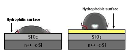
In this project, we chemically modified the surface of thermal silicon dioxide (SiO2) with octatrichlorosilane (OTS), attempting to obtain a desirable interface for the growth of ordered crystalline organic semiconductor thin film. Octatrichlorosilane is an amphiphilic molecule consisting of a long-chain alkyl group (C8H17–) and a polar head group (SiCl3–), which forms Self-Assembled Monolayers (SAMs) on various oxidic substrates. Indicated by contact angle measurements, the surface of thermal SiO2 (θH2O ~ 25°) can be rendered hydrophobic (θH2O ~ 95°) with a lower surface energy by the SAMs. In addition to reducing the surface energy, the alkyl chains standing perpendicular to the gate dielectric surface would cause an out-of-plane preferential orientation of the organic semiconductor molecules at the interface, resulting in improved grain boundaries and increased in-plane π-π stacking. We have observed enhanced charge-carrier mobility of copper tetrabenzoporphyrin (Cu-TBP) by a factor of 3 (0.1 cm2/V/s → 0.3 cm2/V/s) when fabricating devices on octatrichlorosilane surface-treated thermal SiO2 / n++-c-Si substrates. The subthreshold slope (4 V/dec→3 V/dec) and threshold voltage (2V → -1.7V) are also improved after SiO2 surface treatment was performed. The short term goal of this project is to develop full understanding of how the surface treatments of the different gate dielectric surface will affect both the device channel crystallinity and electrical properties, and the long term goal of this project is to replace SAMs by organic thin-film gate dielectrics that could produce similar effects on OTFTs’ properties.
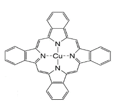
The Cu-TBP used in this project was prepared by Profs. N. Ono and H. Yamada (Ehime University, Japan).

 The crystallinity and crystal orientation of organic semiconductors are closely related to their electrical properties. In organic thin-film transistors (OTFTs), the drain current only travels in a region within approximately 5 to 10 nm of the organic semiconductor / gate dielectric interface. Therefore, the organic semiconductor morphology (or microstructure) at this interface is especially critical to the electrical performance of OTFTs.
 performed. The short term goal of this project is to develop full understanding of how the surface treatments of the different gate dielectric surface will affect both the device channel crystallinity and electrical properties, and the long term goal of this project is to replace SAMs by organic thin-film gate dielectrics that could produce similar effects on OTFTs’ properties.