|

The University of Michigan has a complete clean room facility
with capability to design, fabricate and test organic polymer and
inorganic semiconductor devices and circuits. It is quite likely
that the facilities that are at the disposal of Dr. Kanicki group
constitute the finest aggregation of university-based resources
for Solid-State Electronics in the United States. The processing
and measurements facilities in the Solid-State Electronics Laboratory
(SSEL), augmented by the Organic & Molecular Electronics Laboratory
(OMEL), which has been developed for the research and manufacturing
activities in the area of the Organic & Molecular Electronics, enable
all the research, development, and manufacturing activities conducted
in his group.
Laboratory Space Used by This Group
The following equipment is in place at OMEL:
- Thin film characterization: FTIR (Bio-Rad); single wavelength ellipsometry
(Gaertner); reflectance and UV-visible spectroscopy (Cary 5E), optical microscope
(Nikon)
- Device characterization: two probe stations (Karl Suss and Alessi)
for static and dynamic measurement settings; one cryogenic probe station;
two variable temperature cryostats (Janis); different equipment used for
opto-electronic properties measurements of various thin film device structures
- Electro/Photoluminance measurement system (JY)
- Organic polymer processing tools: spin-coating machine (Solitec), two vacuum
ovens (Blue M), thermal evaporator, multi-chamber dry box with fully integrated
device processing (spin coating, thermal curing and metallization) and measurements
capabilities (MBraun), chemical hood (Fisher), packaging tools (Dymax), UV-curing
system (Electron Lite), UV-ozone treatment system and device inspection station
(Zeiss);
- Device design facility: Sun workstations: Cadence design tool LIQUID,
Sentaurus 2-D device simulator, Design Workshop layout tool, and spectra
simulator systems, etc.
Facilities, Equipment, and Other Resources
|
The Michigan Nanofabrication Facility (MNF) is located in the Electrical Engineering and Computer Science Building and operated by the Solid State Electronics Laboratory. The facility first opened in September 1986 and was fully operational in 1988. It was renamed Michigan Nanofabrication Facility in January 2005. http://www.mnf.umich.edu/
It consists of a Class 1000/100/10 research laboratory with approximately 6,000 square feet of work area and a separate Class 10,000 instructional laboratory of approximately 1,000 square feet which supports formal courses. The research laboratory consists of five process bays (silicon lithography/diffusion, silicon LPCVD, compound semiconductor devices, thin-film deposition, and dry etching) plus five separate, connected rooms for e-beam lithography and metrology (Class 10) and for compound semiconductor materials growth.
The MNF is supported by a lab manager and a staff of 12 engineers and technicians whose primary responsibility is to ensure that the equipment is well maintained and characterized. In addition, the MNF has four staff members whose primary responsibility is to provide training and support users and their projects. The MNF also employs a full time staff engineer for support of the instructional laboratory, which also relies on teaching assistants; graduate students and process engineers for support of the classes. Graduate students perform most of the processing in MNF as part of their doctoral thesis projects. There are also five process engineers who continually process complete devices for specific research projects. The facility is also used by a number of local firms, both large and small, by other universities, and by remote users who can send in their orders to be processed by the laboratory staff.
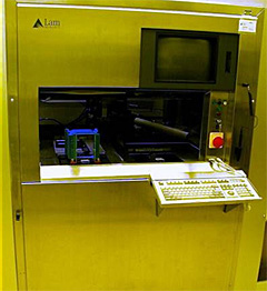
LAM 9000 Reactive Ion Etcher
|  |
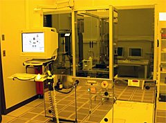
ACS 200 Cluster Tool
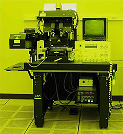
Karl Suss MA-6 Aligner
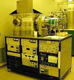
Enerjet Sputter Coater
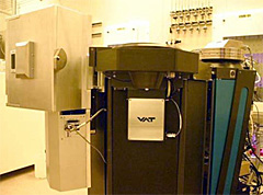
Trion Oracle Reactive Ion Etcher |
|
|
The various SSEL fabrication capabilities are described below:
- Lithography: All of the optical lithography
performed in the SSEL is based on contact aligners
operating in the UV and deep-UV. This equipment includes
Karl Suss MA45 aligners (2) in the Instructional
Laboratory, a Karl Suss MA-6 equipped with infrared
in the silicon bay, and two Karl Suss MJB3 aligners,
one of which is equipped with an excimer laser source
(0.193 micron). An Electronic Vision double-sided
aligner / bonder is also located in this laboratory.
The optical lithography process is well defined at
0.9-micron features. Below that point, a JEOL 5D2F/U
electron-beam lithography system is available for
the direct writing of features to less than 0.10
micron. This system has been operational since late
1986 and has a minimum spot size of 8 nm. This e-beam
lithography system is being upgraded at the present
time to even smaller spot size.
- Diffusion, Oxidation, and LPVD: A total
of 24 Thermco furnaces are available to support high-temperature processes.
Twelve of these are equipped with computer-driven (menu screen) DDC controllers,
providing automatic control of time, temperature, gas sequencing, and
boat insertion / withdrawal. The rest have automatic sequencers for
gas control during the run cycle, with manual control of temperature
and sample loading. All tubes are equipped with all standard process
gases (including TCA for in-situ cleaning), and are equipped to support
four-inch wafers. Wet chemistry benches support the furnaces and spin
dryers dedicated to ensuring proper cleanliness. Cross-contamination
is controlled by dedicating tubes to specific process including wet
and dry oxidation (four tubes), boron (B) and phosphorus (P) pre-deposition
(three tubes), P and B atoms drive-in (two tubes), and contact sintering
(one tube). These processes are duplicated in the eight furnaces in
the Instructional Laboratory, providing valuable backup capability. Three
tubes are dedicated to compound semiconductor processing, and one tube
is used exclusively for polyimide curing. Three of the DDC tubes are
configure for LPCVD, one for oxide / nitride / oxinitride, one for polysilicon,
and one for LTO / PSG. Non-uniformity from the LPCVD
processes is typically less than two percent across a four-inch wafer.
- Materials Growth / Epitaxy: There are several facilities for materials
growth using various forms of epitaxy, including a Riber molecular-beam
epi reactor (MBE), a Varian Gen-II MBE, a Varian metal-organic MBE (MOMBE),
and an Emcore metal-organic CVD (MOCVD) system.
- Thin Film Deposition: The SSEL is well equipped for the vacuum
deposition of a wide variety of materials. A Commonwealth Ion-Beam Milling
and Deposition System, four electron-beam evaporators (two Denton and two
Lesker), a Lesker four-target sputtering system, and a CVC thermal filament
evaporator are on-line for work in this area. A SEMI Group plasma-assisted
PECVD system is also available.
- Etching / Pattern Transfer: Process benches support wet chemistry
to etch a broad range of semiconductors, dielectrics, and metals. The SSEL
also offers a broad range of dry etching capabilities, and many specific
processes have been characterized. Equipment includes an Applied Materials
8300 hexode reactive ion etching system (RIE), a SEMI 1000Tp/C planar dual-chamber
RIE, a SEMI plasma etching system, A Plasma Therm ECR RIE system, a Plasma-
Therm VII Dual Chamber RIE, and a Technics parallel-plate plasma etching
station.
- Metrology: The SSEL has extensive facilities for process characterization
and metrology, including single-wavelength (Geartner Ellipsometer) and
spectroscopic elipsometry (Sopra Ellipsometer), microspectrophotometry,
surface profilometry (Vecco Dektac 8000 and 1600), thin film stress measurements,
DLTS, photoluminescence, high-resolution optical microscopy, and a JOEL
840 scanning electron microscope. In addition, access is also available
to research laboratories such as the Michigan ion Beam Laboratory (MIBL)
and the Electron Microbeam analysis Laboratory (EMAL).
- Bonding and Mounting: The SSEL includes a Hughes VTA-90 split-tip
microwelder, two Kulicke and Soffa ultrasonic wire bonders, and a Kulicke
and Soffa thermocompression bonder. Both a homemade electrostatic wafer
bonding setup and commercial system are available to increase bonding throughput
and yield.
- Computer-Aided Design (CAD): The College of Engineering operates
the Computer aided Engineering Network (CAEN), the backbone of which is
an installation of over 1400 engineering workstations: http://www.engin.umich.edu/caen.
These facilities support virtually the full set of Mentor, Cadence, TMA
and Cascade design automation packages, as well as point tools from other
vendors, providing circuit design, synthesis, layout, simulation, parameter
extraction, verification and tape-out for VLSI circuits, as well as process
and device simulation. Masks are made on our in-house system or by outside
vendors. The Cerius2 version 4.6 molecular modeling software (Molecular
Simulations, Inc.) is also available for this group.
|
The following list of equipment describes facilities available for this research group in Chemistry department:
- Five high-resolution mass spectrometers including electrospray and TOF instruments suitable for characterizing advances intermediates and polymers.
- Infrared microscope and Raman microscope
- Single crystal and powder X-ray diffraction
- Differential scanning calorimetry and thermogravimetric analysis
- Gel permeation chromatography
- Solution (800-300 MHz) and solid state (300 MHz) NMR facilities
The following list of equipment describes facilities presently available for this research group in the Electron Microbeam Analysis Laboratory, Ion Beam Laboratory, Macromolecular Science and Engineering Center and Materials Science and Engineering Department at the University of Michigan: http://www.emal.engin.umich.edu/
- JEOL 4000EX 400 kV high resolution transmission electron microscope (TEM) equipped with a 1024x1024 CCD, with a capability of 0.17 nm point-to-point resolution (Cs=0.8 mm)
- JEOL 2010F 200 kV analytical scanning transmission electron microscope equipped with field emission gun, Gatan Imaging Filter (GIF), cooled multi-scan CCD, and retractable TV rate CCD.
- Philips XL30 Scanning Electron Microscope with Field Emission Gun
- Hitachi S-800 Low Voltage Scanning Electron Microscope
- Hitachi S-520 and S-570 SEM's with Kevex 8000 EDS, with computer control and signal digitizers
- Electroscan E3 Environmental Scanning Electron Microscope
- Digital Instruments Nanoscope III Atomic Force Microscope with Environmental Stage and Multi-mode attachment for STM, Tapping Mode, Lateral Force imaging, Hysitron Picoindentor
- Reichert Ultracut E41 ultramicrotome with FC4E Low Temperature Sectioning Unit and 2.4mm Diatome diamond knife
- Technics, Inc. micro-ion milling unit, Struers Tenupol thinning apparatus and cut-off machine, Southbay Technologies backthinning apparatus, and VCR D-500 dimpler
- Perkin-Elmer PHI 5400 series ESCA/XPS
- Perkin-Elmer PHI 600 Scanning Auger Microprobe
- Rigaku rotating anode X-ray source with WAXS and SAXS cameras and Tennlec position sensitive detector
- Kratky SAXS camera with Braun Position Sensitive Detector
- Bruker X-ray Systems 2D Wire Detector with GADDS software, fine focus copper source, graphite monochromator
- 1.7 MV tandem ion accelerator: duoplasmatron and sputter ion source with UHV beamline and target chamber equipped for RBS, NRA, PIXE, ion channeling, ion implantation, and ion beam mixing
- 2.0 MV Van de Graff accelerator: RF ion source with rapid introduction stage, on-target chamber, equipped for RBS and spectrum analysis
- 400 kV Varian ion implanter with cold cathode ion source for a wide variety of ion species
- Thermal and electron beam evaporator: 3 position 3-beam hearth, thermal evaporation boats, thickness monitor, ion pumping
- Balzers Quadrupole Mass Spectrometer (0-200 amu) with high capacity turbomolecular pump and controlled leak system for continuous sampling from atmospheric or higher pressure systems
- Plasma and Chemical Vapor Deposition reactor system with associated vacuum and detection equipment
|