
Research Archives index
Back Channel Etching Effect on Advanced a-Si:H TFT’s Electrical Properties
Alex Kuo and Jerzy Kanicki
 In order to fabricate an inverted staggered a-Si:H (hydrogenated amorphous silicon) TFT (thin-film transistor), a back channel etch (BCE) is necessary to remove the n+(P-doped) amorphous silicon (n+-a-Si:H) film, plus a fraction of the underlying intrinsic a-Si:H films within channel region just above gate electrode. Our first goal of this project was to find the optimum back channel etching depth of a-Si:H TFT. Secondly we wanted to establish the ideal etching recipe for back channel etch that produces the best advanced a-Si:H TFT in terms of off-current, field-effect mobility, threshold voltage, and sub-threshold swing. We selected four distinct RIE etching gases and a wet etching solution with drastically different etching mechanisms in order to investigate their impact on TFT’s electrical behavior. In order to fabricate an inverted staggered a-Si:H (hydrogenated amorphous silicon) TFT (thin-film transistor), a back channel etch (BCE) is necessary to remove the n+(P-doped) amorphous silicon (n+-a-Si:H) film, plus a fraction of the underlying intrinsic a-Si:H films within channel region just above gate electrode. Our first goal of this project was to find the optimum back channel etching depth of a-Si:H TFT. Secondly we wanted to establish the ideal etching recipe for back channel etch that produces the best advanced a-Si:H TFT in terms of off-current, field-effect mobility, threshold voltage, and sub-threshold swing. We selected four distinct RIE etching gases and a wet etching solution with drastically different etching mechanisms in order to investigate their impact on TFT’s electrical behavior.
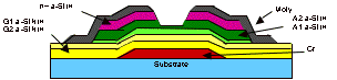
The transistor used in this project consists of a chromium bottom gate, two layers of amorphous silicon nitride as the gate insulator, two layers of a-Si:H as the active layer, a n+ a-Si:H, and molybdenum source/drain contact. In this study four RIE recipes based on different primary etching species, in order of decreasing electron-negativity, were used for the back channel etch process: i) SF6, ii) C2F6, iii) CCl2F2, and iv) HBr. Among the four recipes used, SF6 based chemistry is the most electron-negative, which indicates a high degree of chemical etch mechanism. It is followed by C2F6 and then CCl2F2. Lastly HBr based etching is highly physical, and requires higher ion bombardment than the rest to activate the etching process. Based on literature results, HBr yields the most anistropic etching profile. The RIE recipes will result in different etching profiles in the back channel, as well as different etching mechanisms between the etchant and the target films (n+ a-Si:H and a-Si:H). In addition to dry etching, we performed BCE using wet etching by heated KOH. KOH wet etch is included as a control etch: the entire etch is free of ion and radiation. This allows us to assess the impact of radiation and ion damage to the a-Si:H film quality, thus the electrical performance of the TFT, during RIE BCE process.

Transistors etched with HBr, SF6, and C2F6 show similar field-effect mobility and threshold voltage; however, HBr yields the best device electrical characteristics among dry etchants because of low off-current. We attribute this to the effect of RIE on the back interface density-of-states: HBr etching produces the least amount of back surface states, which results in minimum conduction in the TFT off-regime compared to the rest RIE recipes. Figures above show the linear regime Id-Vgs characteristics of TFT etched by HBr (left) and KOH (right) for different durations of etch back process. We see clearly that field-effect mobility, off-current, and threshold voltage are sensitive to the etching depth of the BCE process. Moreover transistors etched with HBr have higher field-effect mobility than the TFT’s etched with KOH, while they have comparable off- current and threshold voltage. After optimization of both the BCE etchant and the etch back depth, we obtain a-Si:H TFT with field-effect mobility up to 0.91 cm2 V-1 sec-1, threshold voltage of 1.43V, sub-threshold swing of 0.5 V/dec, and off current of 1x10-13 A. This advanced device is acceptable for both AM-LCDs and AM-OLEDs.
This work was done in collaboration and was partially supported by AKT Applied Materials, Inc.
top
|
