
Research Archives Index
Amorphous Metal Oxide Semiconductor Thin-Film Transistors
T. C. (Richard) Fung, Charlene Chang, Kenji Nomura and Jerzy Kanicki
 InGaZnO4 |
Amorphous metal oxide semiconductor (AMOS) is a unique material which is emerging as the new candidate for next generation thin-film transistor (TFT) technology for flat panel displays and imagers. Unlike amorphous-Si, AMOS with properly selecting post-transition-metal cations has shown to have electrical conduction primarily through isotropic s-orbitals. Such conducting mechanism is insensitive to bond angle variance of metal-oxygen-metal chemical bonds induced by structural randomness within AMOS and enables AMOS to have a high mobility even in amorphous phase. Among various AMOS, we choose for our research amorphous InGaZnO4 (a-IGZO), a wide band-gap (~3.2eV) semiconductor. Because it contains a heavy post-transition-metal (primarily In), a-IGZO has a high electron mobility due to the large s-orbital overlap. The existence of Ga helps on suppressing excess electron concentration as well. Therefore, compared to other oxide materials, a-IGZO can be made more intrinsic and is expected to have better semiconductor behavior and stability.
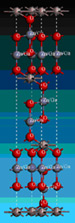
In collaboration with the Tokyo Institute of Technology (Japan), we have studied the fundamental a-IGZO TFT electrical performances of the inverted staggered structure composed of n++Si substrate (gate), thermal SiO2 layer (gate insulator), a-IGZO channel layer and top gold electrodes (source / drain).
 |
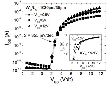 |
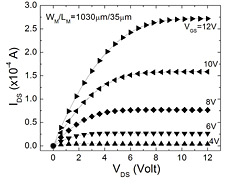
The result shows that 10~12 volt supply voltage is sufficient for a-IGZO TFT operation. Such operating voltage range is significant smaller than the range in a-Si:H TFT (~30V). We can also achieved switching properties comparable to a-Si:H TFT with low off-current (10-11~10-12 A), small subthreshold swing (355mV/dec) and high on/off ratio on the order of 108. The field effect mobility upto 8 cm2V-1s-1 has been observed with the threshold voltage ranging from 1 to 5V. The above device results are suitable for flat-panel displays. We expect the a-IGZO TFT electrical performance can be further improved by proper optimization of the device structure and a-IGZO processing conditions. This project is partially supported by DARPA and Applied Materials Corporation.
top
|
