
Research Archives Index
Electrical Stability of Amorphous InGaZnO Thin-Film Transistors
Tze-Ching Fung and Jerzy Kanicki
During the past few years, there have been great interests in using amorphous In-Ga-Zn-O (a-IGZO) thin-film transistor (TFT) in active-matrix flat panel displays (AM-FPDs). Due to an unique metal s- orbital conduction, a-IGZO TFTs have a higher mobility (μeff)  and steeper sub-threshold swing (S) than traditional covalent bond semiconductors, such as a-Si:H. These properties are highly desirable for next-generation display where higher resolution and faster operating speed are necessary. Today, a-IGZO TFTs have been successfully demonstrated for application like AM-OLED, AM-LCD, electronics paper and transparent electronics. Despite all the progress in a-IGZO TFTs so far, our knowledge of its electrical stability is very li-mited. To ensure a robust product based on a-IGZO TFTs, it is essential to evaluate more in-depth their electrical stability and steeper sub-threshold swing (S) than traditional covalent bond semiconductors, such as a-Si:H. These properties are highly desirable for next-generation display where higher resolution and faster operating speed are necessary. Today, a-IGZO TFTs have been successfully demonstrated for application like AM-OLED, AM-LCD, electronics paper and transparent electronics. Despite all the progress in a-IGZO TFTs so far, our knowledge of its electrical stability is very li-mited. To ensure a robust product based on a-IGZO TFTs, it is essential to evaluate more in-depth their electrical stability
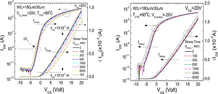
In this project, we studied the bias-temperature stress (BTS) induced electrical insta-bility of RF sputter a-IGZO TFTs. The BTS measurements were performed under different stress voltages (VG_stress) and temperatures. We also monitored the evolution of device degradation by interrupting the BTS at predetermined time steps and mea-suring the TFT transfer properties. A positive shift in TFT Vth was observed under a positive (gate bias) BTS while the Vth shifted to negative for negative BTS. Proper simulation model was proposed to describe experimental data. This research was partially supported by Canon Corp., and Applied Materials Corp.
T.-C. Fung, K. Abe, H. Kumoni, and J. Kanicki, IDW’08, pp.1621-1624 (2008).
top
|
