Modeling of the Current – Voltage Characteristics of Dual-Gate a-InGaZnO Thin Film Transistors
Gwanghyeon Baek and Jerzy Kanicki
A dual-gate (DG) a-InGaZnO (IGZO) thin-film transistor (TFT) structure has both a bottom gate (BG) and a top gate (TG) electrode that can be biased differently. It is well known that the electrical performance of DG TFTs is improved in comparison to single bottom gate TFTs because a larger portion of the channel area is controlled by an additional top gate electrode. Furthermore, it is found that DG a-IGZO TFT has a higher stability under light illumination.
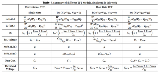
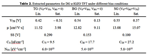
To understand the operation principle of DG a-IGZO TFT, a mathematical analysis based on device physics is needed. In Table 1, we summrize our analysis of the DG a-IGZO TFT’s characteristics for (a) synchronized bias condition, (b) TG condition (BG is biased at 0 V) and (c) BG condition (TG is biased at 0V). Moreover, the TFT parameters of the DG a-IGZO coplanar homo-junction TFT are extracted and compared with the developed analytical model. (Table. 2)