a-InGaZnO Thin-Film Transistors Scaling for High Pixel Density Active Matrix Displays
Gwanghyeon Baek and Jerzy Kanicki
Due to the higher mobility (> 10 cm2/V·s), steeper sub-threshold swing (< 200 mV/Dec.), and long-range uniformity, an amorphous In-Ga-Zn-O (a-IGZO) thin-film transistor (TFT) has received considerable attention in the field of active matrix flat panel display applications (AM-FPD).
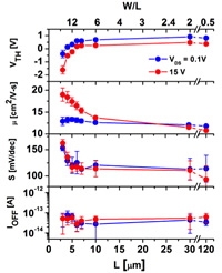
Achieving higher pixel density (> 300 DPI) is one of future technology trends in the area of AM-FPD. It is important to notice that the TFT miniaturization (channel width (W) and length (L) scaling) is a critical limitation for high resolution displays. Also the performance of TFTs is directly influenced by geometrical factors, such as L and W.
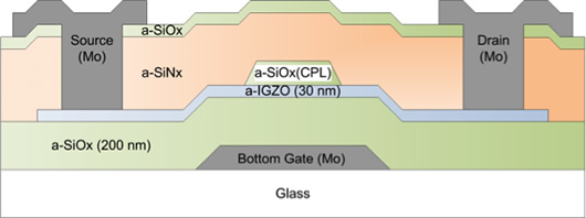
We evaluated the L and W scaling behaviors (see above figure on the right) for coplanar homojunction a-IGZO TFTs. It was previously reported that coplanar homojunction structure has good ohmic source/drain contact, a small parasitic capacitance, and capability of achieving small L. The cross-section of the fabricated TFT is shown in below.

 Due to the higher mobility (> 10 cm2/V·s), steeper sub-threshold swing (< 200 mV/Dec.), and long-range uniformity, an amorphous In-Ga-Zn-O (a-IGZO) thin-film transistor (TFT) has received considerable attention in the field of active matrix flat panel display applications (AM-FPD).